Our group’s equipment
Raman spectrometer: HORIBA T64000
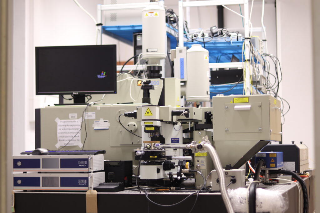
- Laser sources: 325 nm, 442 nm, 532 nm, 633 nm, 785 nm, 1064 nm.
- Tunable laser source: Spectra Physics Matisse 2 Ti-sapphire / dye laser.
- Si CCD and InGaAs detector;
Raman spectrometer: Renishaw
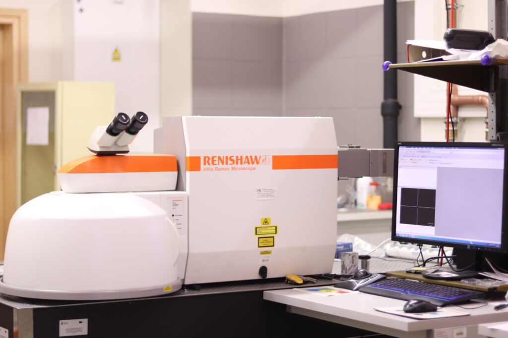
- Laser sources: 532 nm, 633 nm, 785 nm.
FTIR spectrometer: Nicolet iS50
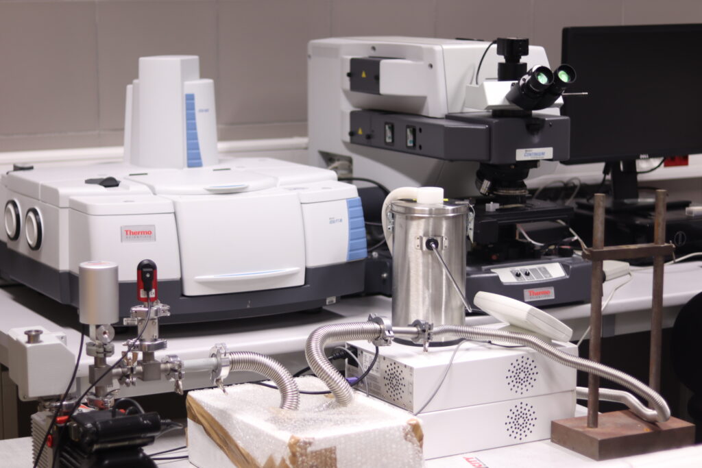
- Measurement range: 15 – 27000 cm-1.
- Possibility of measurements in a wide temperature range.
MOVPE reactor: AIXTRON CCS
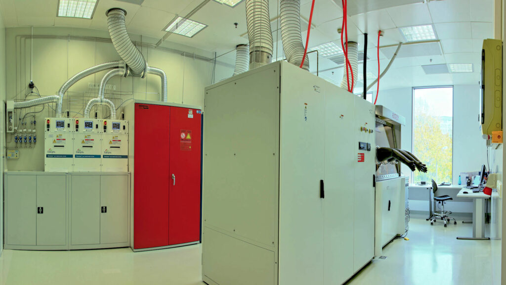
- Closed coupled showerhead reactor for 3 x 2” wafers.
- Reflectometry at a wavelength of 635 nm.
- ARGUS Thermal Mapping System to directly control the substrate temperature.
Wafer Probe System: Agilent B1500 and Cascade Microtech EPS 150 TRIAX
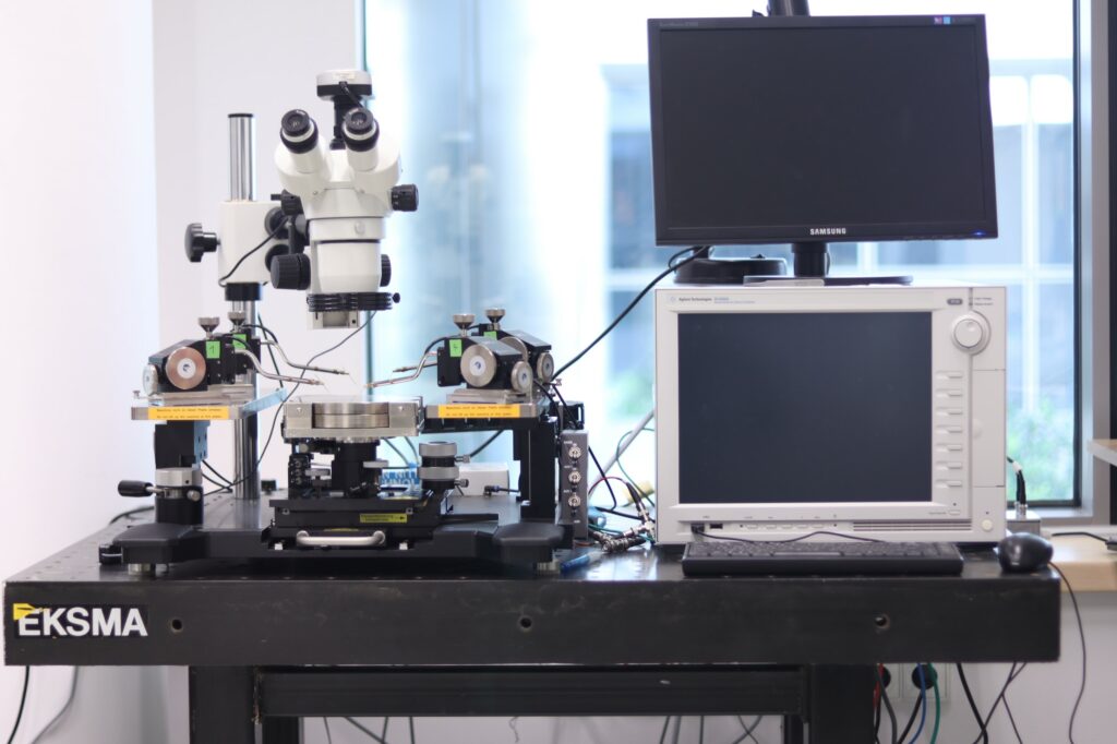
- Tungsten measuring needles.
- Microscope with up to 100x magnification.
- IV and CV measurements.
- Measurement range(IV): 0.1 fA – 1 A and 0.5 μV – 200 V.
Sputtering machine: Gatan pecs model 682
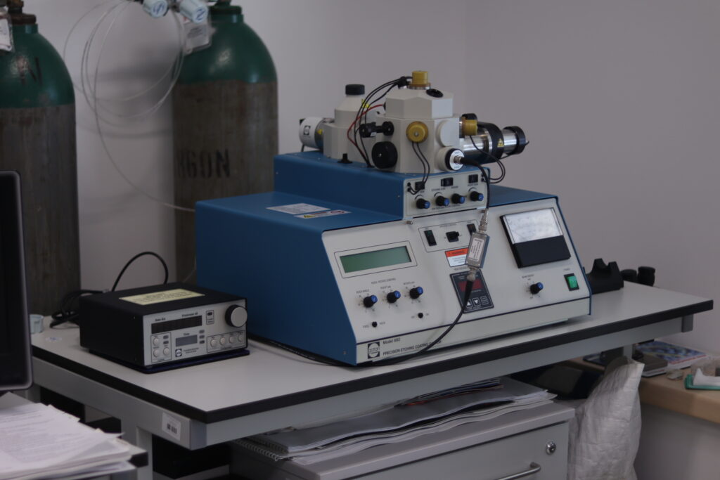
- Uniform coverage over 1 inch.
- Possibility to exchange targets.
- Ion gun allows etching in the area of 7mm – 10mm.
Department equipment
Scanning Electron Microscope (SEM): FEI Helios NanoLab 600
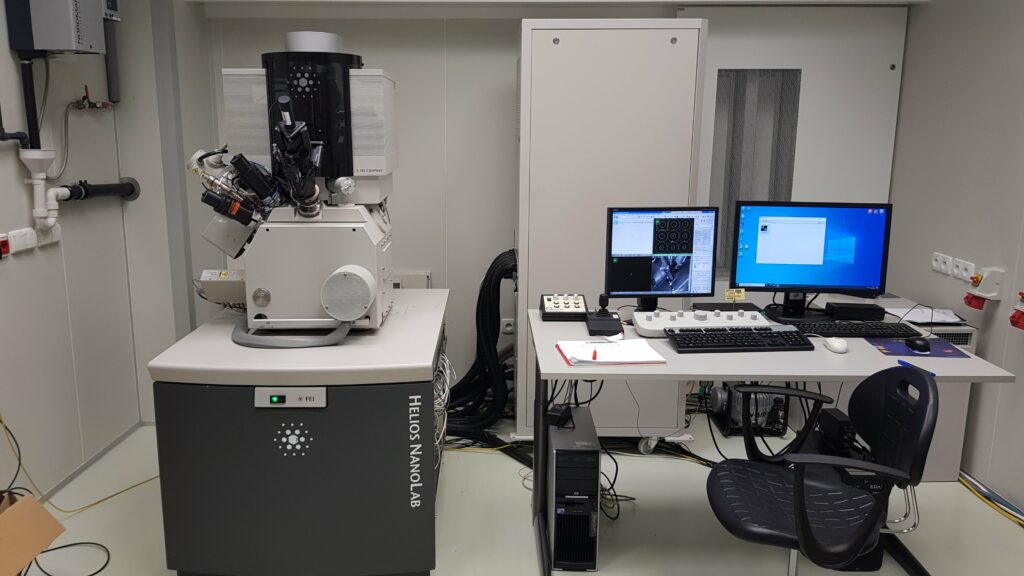
- Electron column with Schottky emitter.
- Resolution up to 1 nm.
- focused ion beam (FIB): with galium source with a resolution of 5 nm.
Maskless Lithography System: POLOS μPrinter
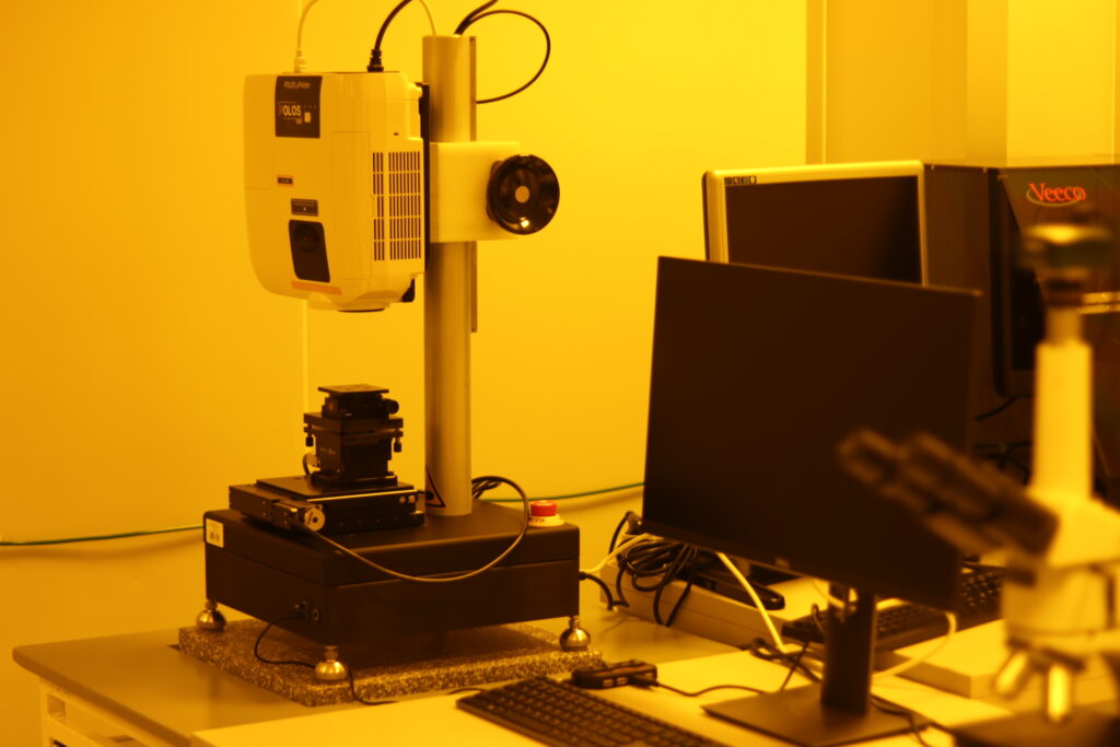
- Lowest resolution down to 2 μm.
- Exposure in: 435 nm.
- Microscope preview: 525 nm.
- Maximum exposure area: 75 x75 mm2.
Furnace: Thermo Scientific™ Vacutherm Vacuum Heating and Drying Ovens
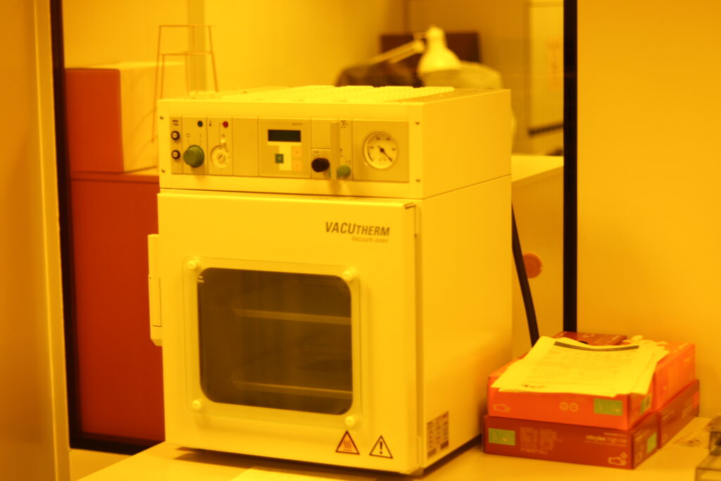
- Possibility of annealing in a vacuum.
- Possibility of heating in nitrogen and other gases.
- Maximum temperature up to 200oC.